- OTHM Level 5: J/650/1143 Research Methods in Health and Social Care
- Feasibility Study for Night Moves: Event Logistics at Finsbury Park, Assignment 2
- EU Law: Dominant Undertakings & EU Four Freedoms – Legal Implications and Market Impact
- BTEC Level 3 Unit 19 Analogue Electronic Devices and Circuits, Assignment 2
- OTHM Level 5 Unit 2 T/650/1139 Managing the Safeguarding and Protection of Vulnerable Individuals
- Legal Analysis of Negligence Claim Against SamsTech for AI Chatbot Errors
- FINA 1007 Research Methods: Assessment Guide & FAQs
- Mathematical Methods in Physics Assignment Question
- Unit 5048 J/650/2990 Sensors and Automation BTEC Level 5
- Transport for London (TfL) Cycle Data Analysis Project – Programming & Data Science
- Sport Coaching Portfolio: Safe, Ethical, and Effective Practices – Assessment 2
- K/507/1406 HSC CM1 Unit 1 Equality, diversity and rights in health and social care, NCFE CACHE Level 3
- MS420/MS508 Advancing Sustainable Development Goals (SDGs) through Business Practices
- C1808 Unit 500 Understanding Leadership and Management in Adult Care – Theories, Styles & Best Practices
- Level 5 Leadership and Management in Adult Care Unit 17, Unit 18 & Unit 16
- Donald Trump’s Statement on South Africa: Economic and Health Impacts
- Level 3 Certificate in Assessing Vocational Achievement (CAVA)
- H/615/1488 Unit 4014: Production Engineering for Manufacture, BTEC Level 4
- CIPD Level 7CO02 People Management: Strategy, Engagement & Technology
- Unit 6: HND Construction Management – Architectural Design and CAD Standards
CE869: Your task for this assignment is to implement a 16 bit CPU To make the assignment feasible within the time frame: High Level Logic Design Assignment, UOE, UK
| University | university of Essex (UOE) |
| Subject | CE869: High Level Logic Design |
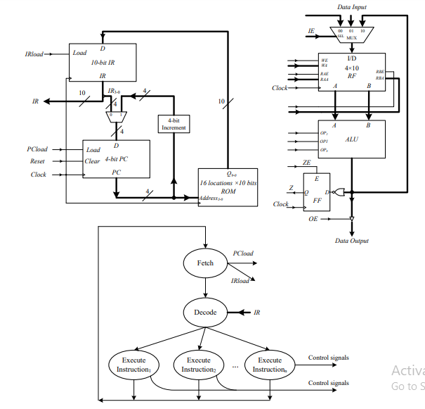
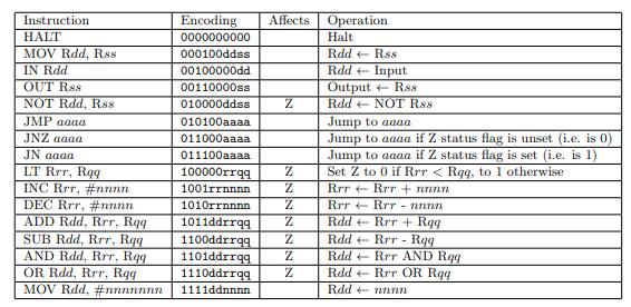
Your task for this assignment is to implement a 16 bit CPU. To make the assignment feasible within the time frame available for this module, the type of CPU will be fairly simple. In particular, the “program sequencing/control flow instruction” datapath can be modeled after the one on the left of Figure 1, while the “arithmetic/logic instruction” datapath can follow a structure like the one on the right in the same figure. Please notice that when RAE and/or RBE is low, the corresponding output(s) will simply match the input “I” to the register file. The opcodes for the instructions that the CPU is required to implement are given in Table 1. You are also required to implement a decode unit in the control unit to interpret the ‘Effects’ and control signals from the output of each instruction.

Figure 1: The figure shows the “program sequencing/control flow instruction” datapath and the “arithmetic/logic instruction” datapath (right).

To test your CPU, you will design the main entity that instantiates the CPU and connects it to the Basys3 peripherals. The sixteen switches of the Basys3 board will represent the input to the CPU while its output will be shown as a hexadecimal number in the four digits of the 7-segment display. The central button will be used as a reset signal to the CPU.
To test the CPU you will be asked to code two programs in the assembly and machine languages of the CPU, implementing the following tasks
- Given a nonzero number N as input, output the sum of the natural numbers less than N;
- Given a number N as input, output “N div 11” (i.e. the integer quotient of the division between N and 11, “TRUNC(N/11)”);
These design specifications should be interpreted as guidelines and should not constrain you from improving the CPU by doing modifications that you think would result in a better “product”. The test programs above, though, should be implemented using only the instructions in Table 1. You are welcome to implement more elaborated programs to test the capabilities and the limitations of the CPU.
Do You Need Assignment of This Question


